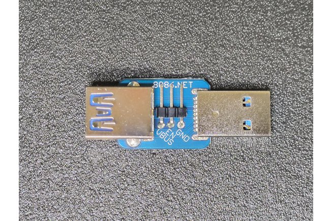
USB3 Power Switch
The USB3 Power Switch is available in two models, Logic Level (LL) and Open Drain (OD). You can switch between either model by altering the solder jumper on the bottom of the PCB.
Logic Level
- ( "PU" solder jumper bridged closest to PCB edge, "OD" solder jumper bridged away from PCB edge )
- The USB Power Switch is normally OFF.
- EN is pulled low to ground by default (see "Pull Up / Pull Down" below).
- Applying a voltage >2V (20V max) to the EN pin turns the power switch on.
- Example: Connect GND (to GND) and EN (to a GPIO) of an Arduino/Raspberry Pi/Pico/etc., set the GPIO pin to be an output and set the pin high to turn the power on.
- Example: Connect the VBUS and EN pins of the power switch to a slide/toggle switch. When the connection is made by the switch, USB power will be turned on.
Open Drain
- ("PU" solder jumper bridged closest to PCB edge, "OD" solder jumper bridged closest to PCB edge)
- The USB Power Switch is normally OFF.
- EN is pulled high to VBUS.
- Using an open drain/open collector signal to pull the EN pin to ground will turn the power switch on.
- Example: Connect GND (to GND) and EN (to a 'Sinking output') on a Pimoroni Automation HAT. Turning the "sink" on will turn USB power on.
- Example: Connect the GND and EN pins of the power switch to a slide/toggle switch. When the connection is made by the switch, USB power will be turned on.
Modifying the PU/OD solder jumpers
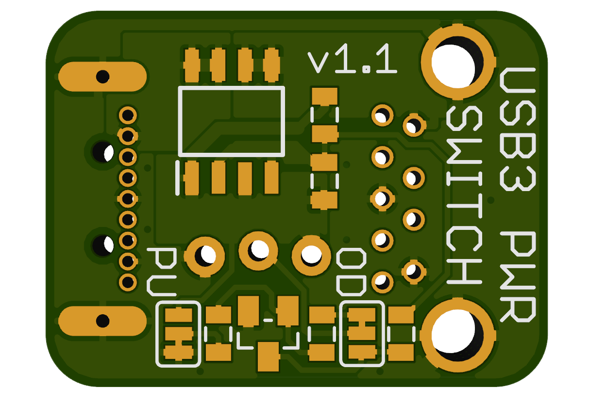
Convert from Open Drain (OD) to Logic Level (LL)
Solder Jumper OD - Remove the solder blob/cut the PCB trace between pad closest to the board edge and middle pad. Then bridge the middle pad to the pad furthest from the board edge.
Pull Up / Pull Down (Logic Level ONLY)
When configured for control using Logic Level the default Pull can be altered. To pull the EN pin LOW (normally off) connect the middle pad to the pad closest to the PCB edge. To pull the EN pin HIGH (normally off) connect the middle pad to the pad furthest from the PCB edge. Irrespective of the LOW/HIGH pull resistor you still need to set the EN pin HIGH to turn the switch on and LOW to turn the switch off.
Convert from Logic Level (LL) to Open Drain (OD)
Solder Jumper OD - Remove the solder blob/cut the PCB trace between pad furthest from the board edge and middle pad. Then bridge the middle pad to the pad closest to the board edge. Solder Jumper PU - MUST be bridged between the middle pad and pad furthest from the PCB edge otherwise the switch will be always on.